
-
PRODUCTS
PRODUCTSThrough continuous technology development and innovation, the company has more than 100 pieces of independent intellectual property rights and patents in core areas such as lidar transmitting and receiving chips, system device and ranging implementation methods.

-
APPLICATION
INDUSTRIESThe company’s core business is mainly divided into two parts. One is the development and production of the vehicle solid-state lidar system and its core chip, the other one is the development and production of 3D sensor and its core chip for consumer electronics. ABAX is committed to provide users with integrated solutions with 3D TOF receiving array chips as the core.

- TECHNICAL SUPPORT
- NEWS
NEWSABAX is committed to provide users with integrated solutions with 3D TOF receiving array chips as the core. The product is mainly used in many intelligent fields such as automatic drive, smartphone and security.
- CAREER
- ABOUT US
ABOUT USNingbo ABAX Sensing Electronic Technology Co., Ltd. was founded in 2016, which is a high-tech company focusing on the research and development of optoelectronic devices, lidar and its core chips. In 2019, the company moved to Ningbo and retained Xi'an as an independent wholly-owned subsidiary company.
- DOWNLOAD

Welcome to ABAX technology support
Hot issues
-
Q
ARead more>>
-
Q
ARead more>>
-
Q
ARead more>>
-
Q
ARead more>>
-
Q
ARead more>>
-
Q
ARead more>>
-
Q
ARead more>>
-
Q
ARead more>>
-
Q
ARead more>>
-
Q
ARead more>>
-
Q
ARead more>>
-
Q
ARead more>>
-
Q
ARead more>>
-
Q
ARead more>>
-
Q
ARead more>>
-
Q
ARead more>>
-
Q
ARead more>>
-
Q
ARead more>>
-
Q
ARead more>>
-
Q
ARead more>>
-
Q
ARead more>>
-
Q
ARead more>>
-
Q
ARead more>>
-
Q
ARead more>>
-
Q
ARead more>>
-
Q
ARead more>>
-
Q
ARead more>>
-
Q
ARead more>>
-
Q
ARead more>>
-
Q
ARead more>>
-
Q
ARead more>>
-
Q
ARead more>>
-
Q
ARead more>>
-
Q
ARead more>>
-
Q
ARead more>>
-
Q
ARead more>>
-
Q
ARead more>>
-
Q
ARead more>>
-
QHow to achieve long-distance detection and interference suppression in Flash mode?
ARead more>>
Problem analysis:
1. A large FOV(Field of View) is required in focal plane array signal receiving due to the principal of Flash surface emission system (as shown in FIG. 1). Thereby, the receiving probability and energy of background light and crosstalk light inside FOV is increased. The invalid signal occupies an extremely proportion in the total signal obtained during the sensor integration process, and the SNR of effective echo energy is reduced (as shown in FIG. 2);
2. Long-distance ranging requires a higher distance detection range. As a result, the dynamic range of the corresponding intrinsic detection light energy will not be less than 80dB. Therefore, the conventional integral receiving array pixel unit which have small dynamic range cannot be applied in the present application.

FIG.1 The ambient light path state in Flash mode. Large FOV improves the receiving probability of “non-self” signal.

FIG.2 The readout SNR of the valid echo signal is reduced by the “non-self” common mode signal introduced in the photoelectric integration process and post-stage circuit noise. It is difficult to obtain an accurate ranging signal.

FIG.3 The well capacity (dynamic range) of the integral capacitor limits the performance. It fails to read out weak signal (long distance) with short exposures; and fails to respond to strong signal (short distance) with long exposures.
ABAX adopts two generations of technology paths to solve those problems above:
★First generation: Pseudo-Random Code Sequence scheme (shown in FIG.4):

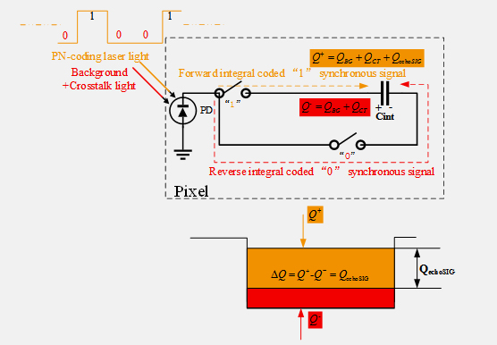
FIG.4 Schematic of ABAX's Photoelectric Integration Method and Background/Crosstalk light suppression.
Solution of eliminate background light and crosstalk light:
Eliminating the "non-self" signal in charge domain at each pixel through the Pixel-Level convolution technology (as shown in FIG. 4). By integrating and outputting the valid "self" signal only, the receiving SNR is increased without increasing transmitting power, and an effective and proper processing of long-distance low-energy echo signals is achieved;
Dynamic range expansion method for long-distance measurements:
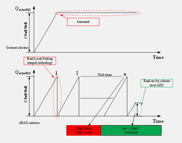
As shown in FIG. 5, using Pixel-Level folding integral technology, the intrinsic dynamic range of pixel is extended. The total number of pixel ADC + column level ADC is increased larger than 18bits, the upper limit saturation point of light intensity receiving is increased.

FIG.5 the Pixel-Level Folding integral extending dynamic range technology.
Second generation: Coherent Detection technology.
The specific technical path is not detailed here. It belongs to technical secret.
If you are interested, you can contact us to further discuss.
Contact email is info@abax-sensing.com.
-
QWhat’s the differences between DTOF and CIS?
ARead more>>
1)Response device:CIS sensor adopts Pinned integral photoelectric device and 4T transistor to realize a pixel, and the analog voltage, and the pixel outputs integrated analog voltage. In DTOF sensor, the SPAD plus quench circuit are generally used to realize the pixel, and the avalanche of the pulse trigger device forms pulse signals. The indicator systems of two response devices are different. CIS pixel focuses on the static indicator system such as QE, DC and FWC, while SPAD has static and dynamic indicators such as PDP, DCR and jitter.
2)Readout form: CIS pixel generally adopts the form of rolling/global shutter, and row selec t column readout.However, DTOF needs to establish multiplexing with TDC circuit to realize address latch and TCSPC readout signals.
3)Data channel bandwidth: D-PHY MIPI can be used to complete data output when CIS is below 100 million pixels. Under the same resolution, the same number of ADC bits and the same frame rate as CIS, ITOF will have at least 4 times more data amount. The amount of DTOF data will increase even larger. So the design of the TOF chip should also focus on the cooperation of the on-chip signal processing technology with improved resolution and high-bandwidth output technology.
-
QCompared with traditional CIS products, what new problems will TOF product development encounter? That is, what are the new problems that traditional CIS manufacturers will encounter when developing TOF?
ARead more>>
As answered in question 1 above, the main new issues include:
1). Improvement of near-infrared quantum efficiency;
2). Isolation crosstalk suppression in the body region;
3). Optimization of vertical electric field and transferred horizontal electric field in the body region;
4). The common mode noise cancellation of the readout circuit loop and the suppression technology of the ranging intrinsic accuracy error caused by nonlinear response;
5). The suppression technology of background light and interference light;
6). The problem of the light receiving dynamic range expansion caused by the increase of the ranging distance;
7). The integration working principle of ITOF determines that there has multi-path interference problems when near-field ranging;
8). The matching problem of TDC multiplexing technology and on-chip processing technology and readout bandwidth in the DTOF technical solution.
Message Feedback
